
In the world of electronics manufacturing, every high-tech gadget, from the smartphone in your pocket to the control systems in a spacecraft, starts its life as a bare PCB. Often referred to as the “blank canvas” of the engineering world, a bare board is the physical platform that provides both the mechanical structure and the electrical pathways for electronic components. Without a high-quality bare PCB, the most sophisticated circuit designs would remain nothing more than theoretical diagrams on a computer screen.
What is a Bare PCB?
A bare PCB is a printed circuit board that has undergone all the fabrication steps—etching, drilling, and plating—but has not yet been populated with electronic components like resistors, capacitors, or microchips. It consists of a non-conductive substrate (usually FR-4) layered with copper traces that act as the “wires” of the system.
While it may look simple to the naked eye, a bare PCB is a marvel of precision engineering. It must meet exact specifications for trace width, hole registration, and surface flatness to ensure that when it finally reaches the assembly line, every component fits and functions perfectly.
The Anatomy of a Bare Board
A standard bare PCB is composed of several critical elements that determine its performance and durability:
- The Substrate: Typically made of fiberglass-reinforced epoxy resin, this provides the board’s rigidity.
- Copper Traces: These are the conductive paths etched onto the substrate. The thickness and width of these traces are calculated to handle specific electrical currents.
- Solder Mask: This is the colorful (usually green, blue, or black) coating that protects the copper from oxidation and prevents “solder bridging” during the assembly process.
- Silkscreen: The white lettering printed on the board. It serves as a map for technicians, indicating where each component should be placed.
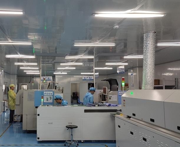
The Critical Importance of Bare Board Testing
Because a bare PCB serves as the foundation for the entire device, any defect at this stage can be catastrophic. If a trace is broken (an open circuit) or two traces are accidentally connected (a short circuit), the final assembled product will fail.
To prevent this, manufacturers employ rigorous testing methods on the bare PCB before it ever leaves the factory:
- Electrical Testing: Using a “flying probe” or a “bed of nails” fixture, the board is checked for continuity and isolation.
- AOI (Automated Optical Inspection): High-resolution cameras scan the board to compare the physical product against the original digital design files, spotting copper defects or etching errors.
- Visual Inspection: Human experts check for cosmetic issues or warping that might affect the board’s structural integrity.
Key Benefits of Starting with a High-Quality Bare PCB
Investing in a premium bare PCB pays dividends throughout the product lifecycle:
1. Reliable Component Soldering
A well-fabricated board features a perfectly flat surface finish (such as ENIG or HASL). This ensures that modern, tiny components—like Ball Grid Arrays (BGAs)—can be soldered with 100% accuracy, reducing the need for expensive rework.
2. Longevity and Durability
Quality substrates and proper plating thickness prevent the board from delaminating or the traces from lifting under thermal stress. This is vital for electronics that must operate in harsh environments.
3. Signal Integrity
In high-speed circuits, the physical dimensions of the bare PCB traces affect the signal speed. Precision etching ensures that impedance is controlled, preventing data corruption or signal loss.
From Prototype to Production
The journey of a bare PCB usually begins with a prototype. Engineers order a small batch of bare boards to verify their circuit logic. Once the design is validated, the process moves to mass production, where thousands of identical boards are fabricated.
At this scale, consistency is the primary goal. Every bare PCB in a batch of 10,000 must be an exact replica of the first, with no variations in hole sizes or copper thickness that could disrupt an automated assembly line.
Conclusion: Securing Your Supply Chain
As electronic devices become more complex and components get smaller, the margin for error in PCB fabrication has shrunk to nearly zero. A microscopic flaw in a bare PCB can lead to thousands of dollars in wasted components and lost time. This is why selecting a partner isn’t just about finding the lowest price—it’s about finding a partner who understands the science of the substrate.
To ensure your next project is built on a flawless foundation, you need to collaborate with an experienced Bare PCB Manufacturer. A manufacturer with a robust quality management system and advanced testing capabilities can provide the peace of mind that every board delivered is ready for assembly and built to last. Whether you are launching a new consumer electronic or a mission-critical industrial tool, the quality of your bare board is the quality of your brand.